In the semiconductor manufacturing field, the traditional large-scale, high-capital investment manufacturing model is facing a potential revolution. With the upcoming "CEATEC 2024" exhibition, the Minimum Wafer Fab Promotion Organization is showcasing a brand-new semiconductor manufacturing method that utilizes ultra-small semiconductor manufacturing equipment for lithography processes. This innovation is bringing unprecedented opportunities for small and medium-sized enterprises (SMEs) and startups. This article will synthesize relevant information to explore the background, advantages, challenges, and potential impact of minimum wafer fab technology on the semiconductor industry.
Semiconductor manufacturing is a highly capital- and technology-intensive industry. Traditionally, semiconductor manufacturing requires large factories and clean rooms to mass-produce 12-inch wafers. The capital investment for each large wafer fab often reaches up to 2 trillion yen (approximately 120 billion RMB), making it difficult for SMEs and startups to enter this field. However, with the emergence of minimum wafer fab technology, this situation is changing.

Minimum wafer fabs are innovative semiconductor manufacturing systems that use 0.5-inch wafers, significantly reducing production scale and capital investment compared to traditional 12-inch wafers. The capital investment for this manufacturing equipment is only about 500 million yen (approximately 23.8 million RMB), enabling SMEs and startups to begin semiconductor manufacturing with a lower investment.
The origins of minimum wafer fab technology can be traced back to a research project initiated by the National Institute of Advanced Industrial Science and Technology (AIST) in Japan in 2008. This project aimed to create a new trend in semiconductor manufacturing by achieving multi-variety, small-batch production. The initiative, led by Japan's Ministry of Economy, Trade and Industry, involved collaboration among 140 Japanese companies and organizations to develop a new generation of manufacturing systems, aiming to significantly reduce costs and technical barriers, allowing automotive and home appliance manufacturers to produce the semiconductors and sensors they need.
**Advantages of Minimum Wafer Fab Technology:**
1. **Significantly Reduced Capital Investment:** Traditional large wafer fabs require capital investments exceeding hundreds of billions of yen, while the target investment for minimum wafer fabs is only 1/100 to 1/1000 of that amount. Since each device is small, there is no need for large factory spaces or photomasks for circuit formation, greatly reducing operational costs.
2. **Flexible and Diverse Production Models:** Minimum wafer fabs focus on manufacturing a variety of small-batch products. This production model allows SMEs and startups to quickly customize and produce according to their needs, meeting the market demand for customized and diverse semiconductor products.
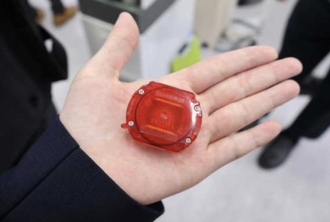
3. **Simplified Production Processes:** The manufacturing equipment in minimum wafer fabs has the same shape and size for all processes, and the wafer transport containers (shuttles) are universal for each step. Since the equipment and shuttles operate in a clean environment, there is no need to maintain large clean rooms. This design significantly reduces manufacturing costs and complexity through localized clean technology and simplified production processes.
4. **Low Power Consumption and Household Power Use:** The manufacturing equipment in minimum wafer fabs also features low power consumption and can operate on standard household AC100V power. This characteristic allows these devices to be used in environments outside of clean rooms, further reducing energy consumption and operational costs.
5. **Shortened Manufacturing Cycles:** Large-scale semiconductor manufacturing typically requires a long wait time from order to delivery, while minimum wafer fabs can achieve on-time production of the required quantity of semiconductors within the desired timeframe. This advantage is particularly evident in fields like the Internet of Things (IoT), which require small, high-mix semiconductor products.
**Demonstration and Application of Technology:**
At the "CEATEC 2024" exhibition, the Minimum Wafer Fab Promotion Organization demonstrated the lithography process using ultra-small semiconductor manufacturing equipment. During the demonstration, three machines were arranged to showcase the lithography process, which included resist coating, exposure, and development. The wafer transport container (shuttle) was held in hand, placed into the equipment, and activated with the press of a button. After completion, the shuttle was picked up and set on the next device. The internal status and progress of each device were displayed on their respective monitors.
Once these three processes were completed, the wafer was inspected under a microscope, revealing a pattern with the words "Happy Halloween" and a pumpkin illustration. This demonstration not only showcased the feasibility of minimum wafer fab technology but also highlighted its flexibility and high precision.
Additionally, some companies have begun to experiment with minimum wafer fab technology. For example, Yokogawa Solutions, a subsidiary of Yokogawa Electric Corporation, has launched streamlined and aesthetically pleasing manufacturing machines, roughly the size of a beverage vending machine, each equipped with functions for cleaning, heating, and exposure. These machines effectively form a semiconductor manufacturing production line, and the minimum area required for a "mini wafer fab" production line is only the size of two tennis courts, just 1% of the area of a 12-inch wafer fab.
However, minimum wafer fabs currently struggle to compete with large semiconductor factories. Ultra-fine circuit designs, especially in advanced process technologies (such as 7nm and below), still rely on advanced equipment and large-scale manufacturing capabilities. The 0.5-inch wafer processes of minimum wafer fabs are more suitable for manufacturing relatively simple devices, such as sensors and MEMS.
Minimum wafer fabs represent a highly promising new model for semiconductor manufacturing. Characterized by miniaturization, low cost, and flexibility, they are expected to provide new market opportunities for SMEs and innovative companies. The advantages of minimum wafer fabs are particularly evident in specific application areas such as IoT, sensors, and MEMS.
In the future, as the technology matures and is promoted further, minimum wafer fabs could become an important force in the semiconductor manufacturing industry. They not only provide small businesses with opportunities to enter this field but may also drive changes in the cost structure and production models of the entire industry. Achieving this goal will require more efforts in technology, talent development, and ecosystem building.
In the long run, the successful promotion of minimum wafer fabs could have a profound impact on the entire semiconductor industry, particularly in terms of supply chain diversification, manufacturing process flexibility, and cost control. The widespread application of this technology will help drive further innovation and progress in the global semiconductor industry.
Post time: Oct-14-2024

