

Deep within the supply chain, some magicians turn sand into perfect diamond-structured silicon crystal discs, which are essential to the entire semiconductor supply chain. They are part of the semiconductor supply chain that increases the value of "silicon sand" by nearly a thousand times. The faint glow you see on the beach is silicon. Silicon is a complex crystal with brittleness and solid-like metal (metallic and non-metallic properties). Silicon is everywhere.
Silicon is the second most common material on Earth, after oxygen, and the seventh most common material in the universe. Silicon is a semiconductor, meaning it has electrical properties between conductors (such as copper) and insulators (such as glass). A small amount of foreign atoms in the silicon structure can fundamentally change its behavior, so the purity of semiconductor-grade silicon must be astonishingly high. The acceptable minimum purity for electronic-grade silicon is 99.999999%.
This means that only one non-silicon atom is allowed for every ten billion atoms. Good drinking water allows for 40 million non-water molecules, which is 50 million times less pure than semiconductor-grade silicon.
Blank silicon wafer manufacturers must convert high-purity silicon into perfect single-crystal structures. This is done by introducing a single mother crystal into molten silicon at the appropriate temperature. As new daughter crystals begin to grow around the mother crystal, the silicon ingot slowly forms from the molten silicon. The process is slow and may take a week. The finished silicon ingot weighs about 100 kilograms and can make over 3,000 wafers.
The wafers are cut into thin slices using very fine diamond wire. The precision of the silicon cutting tools is very high, and operators must be constantly monitored, or they will start using the tools to do silly things to their hair. The brief introduction to the production of silicon wafers is too simplified and does not fully credit the geniuses' contributions; but it is hoped to provide a background for a deeper understanding of the silicon wafer business.
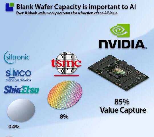
The supply and demand relationship of silicon wafers
The silicon wafer market is dominated by four companies. For a long time, the market has been in a delicate balance between supply and demand.
The decline in semiconductor sales in 2023 has led the market to be in a state of oversupply, causing chip manufacturers' internal and external inventories to be high. However, this is only a temporary situation. As the market recovers, the industry will soon return to the edge of capacity and must meet the additional demand brought about by the AI revolution. The transition from traditional CPU-based architecture to accelerated computing will have an impact on the entire industry, as However, this may have an impact on the low-value segments of the semiconductor industry.
Graphics Processing Unit (GPU) architectures require more silicon area
As the demand for performance increases, GPU manufacturers must overcome some design limitations to achieve higher performance from GPUs. Obviously, making the chip larger is one way to achieve higher performance, as electrons do not like to travel long distances between different chips, which limits performance. However, there is a practical limitation to making the chip larger, known as the "retina limit".
The lithography limit refers to the maximum size of a chip that can be exposed in a single step in a lithography machine used in semiconductor manufacturing. This limitation is determined by the maximum magnetic field size of the lithography equipment, especially the stepper or scanner used in the lithography process. For the latest technology, the mask limit is usually around 858 square millimeters. This size limitation is very important because it determines the maximum area that can be patterned on the wafer in a single exposure. If the wafer is larger than this limit, multiple exposures will be needed to fully pattern the wafer, which is impractical for mass production due to complexity and alignment challenges. The new GB200 will overcome this limitation by combining two chip substrates with particle size limitations into a silicon interlayer, forming a super-particle-limited substrate that is twice as large. Other performance limitations are the amount of memory and the distance to that memory (i.e. memory bandwidth). New GPU architectures overcome this problem by using stacked high-bandwidth memory (HBM) that is installed on the same silicon interposer with two GPU chips. From a silicon perspective, the problem with HBM is that each bit of silicon area is twice that of traditional DRAM due to the high-parallel interface required for high bandwidth. HBM also integrates a logic control chip into each stack, increasing the silicon area. A rough calculation shows that the silicon area used in 2.5D GPU architecture is 2.5 to 3 times that of the traditional 2.0D architecture. As mentioned earlier, unless foundry companies are prepared for this change, silicon wafer capacity may become very tight again.
Future capacity of the silicon wafer market
The first of the three laws of semiconductor manufacturing is that the most money needs to be invested when the least amount of money is available. This is due to the industry's cyclical nature, and semiconductor companies have a hard time following this rule. As shown in the figure, most silicon wafer manufacturers have recognized the impact of this change and have almost tripled their total quarterly capital expenditures in the past few quarters. Despite the difficult market conditions, this is still the case. What is even more interesting is that this trend has been going on for a long time. Silicon wafer companies are fortunate or know something that others don't. The semiconductor supply chain is a time machine that can predict the future. Your future may be someone else's past. While we don't always get answers, we almost always get worthwhile questions.
Post time: Jun-17-2024