

In the fast-paced world of electronics manufacturing, the need for innovative packaging solutions has never been greater. As electronic components become smaller and more delicate, the demand for reliable and efficient packaging materials and designs has increased. Carrier tape, a widely used packaging solution for electronic components, has evolved to meet these demands, offering enhanced protection and precision in electronics packaging.
The materials used in carrier tape play a crucial role in ensuring the safety and integrity of electronic components during storage, transportation, and assembly. Traditionally, carrier tapes were made from materials such as polystyrene, polycarbonate, and PVC, which provided basic protection but had limitations in terms of durability and environmental impact. However, with advancements in material science and engineering, new and improved materials have been developed to address these limitations.
One of the key innovations in carrier tape materials is the use of conductive and static-dissipative materials, which help to protect sensitive electronic components from electrostatic discharge (ESD) and electromagnetic interference (EMI). These materials provide a shield against static electricity and external electromagnetic fields, safeguarding the components from potential damage during handling and transportation. Additionally, the use of antistatic materials in carrier tape manufacturing ensures that the components remain safe from static charges, which can compromise their performance and reliability.
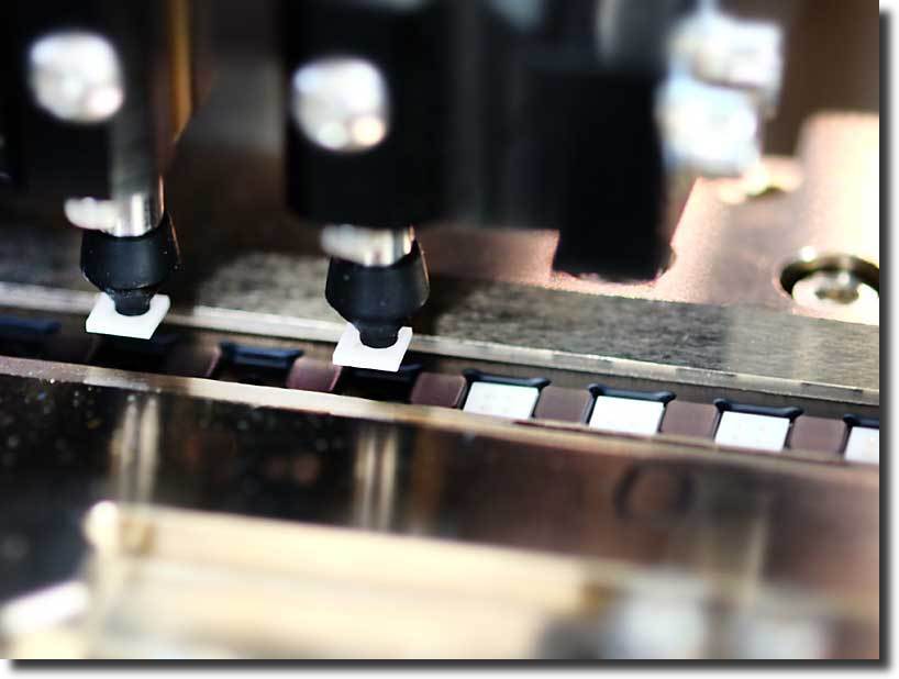
Furthermore, the design of carrier tape has also undergone significant advancements to enhance its protective and precision capabilities. The development of embossed carrier tape, featuring pockets or compartments for individual components, has revolutionized the way electronic components are packaged and handled. This design not only provides a secure and organized arrangement for the components but also allows for precise pick-and-place operations during assembly, reducing the risk of damage and misalignment.
In addition to protection, precision is a critical factor in electronics packaging, especially in automated assembly processes. The design of carrier tape now incorporates features such as accurate pocket dimensions, precise pitch spacing, and advanced sealing techniques to ensure the secure and precise placement of components. This level of precision is essential for high-speed assembly equipment, where even the slightest deviation can lead to production errors and component damage.
Moreover, the environmental impact of carrier tape materials and design has also been a focus of innovation. With the growing emphasis on sustainability and eco-friendly practices, manufacturers have been exploring biodegradable and recyclable materials for carrier tape production. By incorporating these materials into the design, the electronics industry can reduce its carbon footprint and contribute to a more sustainable supply chain.
In conclusion, the evolution of carrier tape materials and design has brought about significant advancements in the protection and precision of electronics packaging. The use of advanced materials, such as conductive and static-dissipative compounds, has enhanced the safety of electronic components, while innovative designs, such as embossed carrier tape, have improved the precision and efficiency of assembly processes. As the electronics industry continues to evolve, the ongoing innovation in carrier tape materials and design will play a crucial role in meeting the demands for reliable, sustainable, and high-performance packaging solutions.
Post time: May-18-2024